Table of Contents
- Why Is Polysilicon Testing Necessary?
- What Purity Grades Define Solar vs Semiconductor Polysilicon?
- How Are Trace Metal Impurities Tested (ICP-MS)?
- How Are Carbon and Oxygen Measured (FTIR)?
- How Is Minority Carrier Lifetime Measured (μ-PCD)?
- How Is Resistivity Measured (Four-Point Probe)?
- Which Standards Govern Polysilicon (GB/T 12963, SEMI PV17)?
- FAQ
- Our Polysilicon material testing Capabilities
Why Is Polysilicon Testing Necessary?
Polysilicon is the feedstock for two of the most purity-sensitive industries on earth — photovoltaic cells and semiconductor chips — and its purity, measured in "nines" from 6N to 11N, directly sets device efficiency, yield, and reliability. A single trace contaminant at parts-per-billion-atomic (ppba) concentration can degrade a solar cell's short-circuit current, shorten a chip transistor's minority carrier lifetime, or trigger a leakage-current failure. Testing exists because these defects are invisible without analytical chemistry: you cannot see a 0.002 ppba copper contamination with the naked eye, but it raises a wafer's local leakage current and reduces module output over its 25-year service life.
The practical stake is economic. Upgrading polysilicon from 6N to 8N purity lowers the photovoltaic wafer defect rate measurably, and semiconductor-grade 11N material — where no more than one impurity atom is tolerated per 100 billion silicon atoms — is the entry ticket to advanced node chip manufacturing. Testing is how a producer proves a lot meets its grade, how a buyer verifies a supplier's claim, and how a fab traces a yield loss back to a contaminated feedstock batch. Every polysilicon lot that enters a cell line or a fab has been characterized by the test methods below.
What Purity Grades Define Solar vs Semiconductor Polysilicon?
Polysilicon purity is expressed in "nines" (N), where each N is one additional 9 in the percentage. The industry splits into two grade tiers that differ by roughly three orders of magnitude in allowable impurity:
| Grade | Purity | Equivalent | Typical Application |
|---|---|---|---|
| Solar grade | 6N – 8N | 99.9999% – 99.999999% | Photovoltaic cells |
| Semiconductor / electronic grade | ≥ 9N, up to 11N | 99.999999999% (11N) | Integrated circuit chips |
The 11N semiconductor-grade threshold is austere: it permits no more than one impurity atom per 100 billion silicon atoms. Crossing from solar to semiconductor grade is not a gradual improvement — it requires a fundamentally tighter purification chain (multi-stage distillation of trichlorosilane, CVD deposition at 1050–1100 °C, and hydrogen reduction), and the cost scales accordingly. Testing must distinguish these grades with methods sensitive enough to resolve impurity concentrations five to six orders of magnitude below the bulk — which is why ICP-MS, not gravimetric chemistry, is the workhorse method at these levels.
How Are Trace Metal Impurities Tested (ICP-MS)?
inductively coupled plasma mass spectrometry (ICP-MS) is the primary method for quantifying trace metal contamination in polysilicon, because it can measure up to 31 metallic elements simultaneously at parts-per-trillion (ppt) detection limits. The method works by dissolving the silicon sample in a high-purity hydrofluoric acid matrix, ionizing the resulting solution in an argon plasma, and separating the ions by mass-to-charge ratio — so each metal is identified and quantified against its calibration curve.
The impurity thresholds that define a compliant lot are at ppba (parts per billion atomic) levels, far below what wet chemistry can resolve:
| Impurity | Typical Upper Limit |
|---|---|
| Iron (Fe) | ≤ 0.01 ppba |
| Aluminum (Al) | < 0.005 ppba |
| Copper (Cu) | ≤ 0.002 ppba |
| Titanium / Vanadium (Ti / V) | ≤ 0.001 ppba |
| Interstitial oxygen | ≤ 5 × 10¹⁷ atoms/cm³ |
| Carbon | ≤ 0.3 ppm |
These limits exist because each metal harms device physics in a specific way. Copper diffuses rapidly through the silicon lattice and, once present above 0.002 ppba, raises the wafer's local leakage current. Iron and titanium act as recombination centers: each 0.05 ppba increment raises the carrier recombination rate and reduces the solar cell's short-circuit current density. The practical downstream effect — verified by long-term module studies — is that strict metal blocking lowers a solar module's annual power degradation from ~0.7% to ~0.45%, which over a 25-year service life and a utility-scale farm is a material revenue difference. This is why ICP-MS is run on every polysilicon lot, not just on audit samples.
How Are Carbon and Oxygen Measured (FTIR)?
Fourier-transform infrared spectroscopy (FTIR) measures the carbon and oxygen content of polysilicon by scanning the sample across a wavenumber range of 400–4000 cm⁻¹ and resolving the characteristic absorption peaks of carbon-oxygen bonds. Typical instrumentation achieves a carbon-oxygen resolution precision of 0.5 cm⁻¹, sufficient to quantify concentrations at the ppm level required by the grade specification.
The reason carbon and oxygen are controlled, not just metals, is their role in defect formation. Carbon accelerates oxygen-precipitate formation in the crystal, which induces secondary defects that degrade minority carrier lifetime — the same lifetime that sets chip switching speed and solar cell efficiency. Oxygen is limited because interstitial oxygen (≤ 5 × 10¹⁷ atoms/cm³) forms thermal donors during high-temperature processing that shift the wafer's resistivity off target. FTIR therefore complements ICP-MS: where ICP-MS tracks metals, FTIR tracks the light elements (C, O) that ICP-MS handles poorly, and together they cover the impurity panel a grade specification demands.
How Is Minority Carrier Lifetime Measured (μ-PCD)?
Minority carrier lifetime is the average time an excess minority carrier (electron in p-type, hole in n-type) survives before recombining, and it is one of the most sensitive integrated indicators of polysilicon purity — because impurities create recombination centers that shorten it. The standard measurement method is microwave photoconductance decay (μ-PCD): a laser pulse generates excess carriers in the sample, and a microwave probe measures the decay of photoconductance as those carriers recombine; the time constant of the decay is the lifetime.
The correlation between purity grade and lifetime is direct and steep:
| Polysilicon Grade | Typical Minority Carrier Lifetime |
|---|---|
| 6N (solar) | ~50 μs |
| 8N (high solar / low electronic) | ~200 – 250 μs |
| Electronic grade (≥ 9N) | Higher, dopant-dependent |
Because lifetime is degraded by the very metals and defects that ICP-MS and FTIR measure individually, μ-PCD functions as the integrated "pass/fail" screen: a lot with lifetime well below the grade's expected value flags a contamination problem even if no single impurity individually exceeds its limit. This makes μ-PCD the fastest lot-acceptance test — a single measurement exposes the cumulative effect of all recombination centers. Research has shown that reducing surface metals on polysilicon from 20–200 ppbw to below 10 ppbw raises the resulting Czochralski crystal's minority carrier lifetime substantially, confirming the causal chain from feedstock purity through device performance.
How Is Resistivity Measured (Four-Point Probe)?
Resistivity is the bulk electrical resistance normalized to geometry, and in polysilicon it is governed by dopant type and concentration. The measurement method is the four-point probe: four collinear contacts are pressed onto the sample surface, current passes through the outer two, and the voltage drop is measured across the inner two — eliminating contact resistance from the reading. The result, in Ω·cm, is then mapped against the dopant specification.
The resistivity windows for the two dopant types are: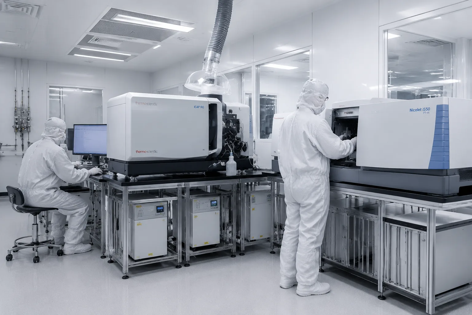
| Dopant Type | Typical Resistivity Range | Batch Uniformity |
|---|---|---|
| P-type (boron-doped) | 0.5 – 3.0 Ω·cm | Standard deviation < 0.1 Ω·cm |
| N-type (phosphorus-doped) | 1 – 5 Ω·cm | Batch dispersion < 2.5% |
Resistivity matters because it sets the wafer's baseline electrical behavior that every downstream device process assumes. A lot whose resistivity drifts outside the window forces the fab to re-tune its process — or reject the lot. Because resistivity is sensitive to both intentional dopants and unintentional contaminants (thermal donors from oxygen, acceptors from boron contamination), a four-point probe map that shows drift or radial non-uniformity is an early warning of a contamination or crystal-growth problem, often before it shows up in device yield.
Which Standards Govern Polysilicon (GB/T 12963, SEMI PV17)?
Polysilicon testing is governed by both Chinese national standards and the international SEMI framework, and the two systems cover slightly different scope:
| Standard | Title | Scope | Status |
|---|---|---|---|
| GB/T 12963-2022 | Electronic-grade polycrystalline silicon | Designations, technical requirements, test methods, inspection rules for electronic-grade polysilicon (chlorosilane/silane route) | ✅ Current (effective 2023-07-01) |
| GB/T 25074-2017 | Solar-grade polycrystalline silicon | Solar-grade polysilicon specifications | ⚠️ Withdrawn (verify replacement) |
| SEMI PV17 | Virgin Silicon Feedstock Materials for Photovoltaic Applications | Specification for PV-grade virgin silicon feedstock (CVD, metallurgical, other routes) | Current |
| SEMI M1 | Specifications for Polished Monocrystalline Silicon Wafers | Downstream polished wafer spec (semiconductor) | Current |
For the Chinese market, GB/T 12963-2022 is the operative standard for electronic-grade material — it defines what a compliant electronic-grade lot must contain and which test methods to use. Note that GB/T 25074-2017 (solar-grade) has been withdrawn; solar-grade material is now typically qualified against SEMI PV17 or the replacement national standard. The SEMI standards govern the international trade flow: a lot destined for a global PV buyer is qualified to SEMI PV17, while one destined for a Chinese fab is qualified to GB/T 12963-2022. A complete characterization report for a globally traded lot carries both.
FAQ
What is the difference between solar-grade and semiconductor-grade polysilicon?
Solar-grade polysilicon is 6N–8N pure (99.9999%–99.999999%); semiconductor (electronic) grade is ≥9N, up to 11N (99.999999999%). The 11N threshold allows no more than one impurity atom per 100 billion silicon atoms. Semiconductor grade requires a tighter purification chain and costs substantially more; testing must resolve impurities 100–1000× lower than solar grade.
Why is ICP-MS used instead of chemical titration for polysilicon?
Because the impurity thresholds are at ppba (parts per billion atomic) and ppt levels — far below what wet chemistry can resolve. ICP-MS ionizes the dissolved sample in an argon plasma and separates ions by mass, achieving 0.001 ppt detection limits for up to 31 metals simultaneously. Titration cannot reach the sensitivity required for 8N–11N material.
What minority carrier lifetime should good polysilicon achieve?
It scales with purity: 6N solar grade typically measures ~50 μs; 8N high-purity material reaches ~200–250 μs. Electronic grade exceeds these values, depending on dopant. Lifetime is measured by microwave photoconductance decay (μ-PCD) and is the most sensitive integrated indicator of purity, because every recombination-center impurity shortens it.
How are carbon and oxygen tested, and why do they matter?
Carbon and oxygen are measured by FTIR (Fourier-transform infrared) at 400–4000 cm⁻¹ with ~0.5 cm⁻¹ resolution. Carbon accelerates oxygen-precipitate defects that degrade minority carrier lifetime; interstitial oxygen forms thermal donors that shift resistivity. Limits: carbon ≤ 0.3 ppm, oxygen ≤ 5 × 10¹⁷ atoms/cm³.
Which standard applies to electronic-grade polysilicon in China?
GB/T 12963-2022 (Electronic-grade polycrystalline silicon) is the current operative standard, effective 2023-07-01. Note that GB/T 25074-2017 (solar-grade) has been withdrawn. For international PV trade, SEMI PV17 governs virgin silicon feedstock.
Can polysilicon testing trace a yield loss back to a contaminated lot?
Yes. Because ICP-MS quantifies specific metals, FTIR quantifies carbon/oxygen, and μ-PCD integrates their combined effect on lifetime, a characterization report can correlate a fab's yield loss to a specific feedstock batch's impurity profile. The traceability is strongest when every lot is characterized on intake — which is standard practice for both solar and semiconductor supply chains.
Our Polysilicon Material Testing Capabilities
Beijing ZKGX Research Institute provides third-party analytical testing for solar-grade and electronic-grade polysilicon. Our testing follows the validated methods and the GB/T 12963-2022 / SEMI PV17 frameworks, applied to each lot's grade and intended application.
Standards / Methods Our Testing Covers
| Test Endpoint | Method Reference |
|---|---|
| Electronic-grade polysilicon | GB/T 12963-2022 |
| Virgin PV silicon feedstock | SEMI PV17 |
| Trace metal impurities (up to 31 elements) | ICP-MS |
| Carbon and oxygen content | FTIR (400–4000 cm⁻¹) |
| Minority carrier lifetime | μ-PCD (microwave photoconductance decay) |
| Resistivity (P-type / N-type) | Four-point probe |
| Defect density mapping | Photoluminescence (PL, 532 nm) |
What We Can Test
- Solar-grade polysilicon (6N–8N) — full purity and electrical characterization for cell-line intake
- Electronic-grade polysilicon (≥9N) — ppba-level impurity screening for fab qualification
- Czochralski / ingot feedstock — resistivity, lifetime, and metal-content verification before crystal growth
- Granular and chunk polysilicon — both CVD-rod and FBR-granule forms
Sample Types We Accept
Chunk, granule, and rod-section polysilicon samples in contamination-controlled packaging. ICP-MS samples are dissolved in a high-purity HF matrix; FTIR and resistivity tests use polished or as-cut sections per the method standard.
Get a Testing Quote
If you need to qualify a polysilicon lot for a solar cell line or a semiconductor fab — or trace a yield loss to a contaminated feedstock — our team will confirm the applicable standard, sample requirements, and a quotation. Contact Beijing ZKGX Research Institute to start.