Table of Contents
- What does photoresist testing cover?
- How is film thickness measured after spin coating?
- How are viscosity and solids content determined?
- How is the contrast curve and dose-to-clear measured?
- How is dissolution rate characterized?
- How are resolution and sidewall profile qualified?
- How is residual photoresist detected after stripping?
- FAQ
- Our photoresist testing service
What does photoresist testing cover?
Photoresist testing is not a single property measurement; it is a programme that spans the liquid resist (as supplied in the bottle), the coated film (after spin coating and bake), the exposed-and-developed pattern (after lithographic processing), and the stripped wafer (after the resist is removed). Each stage answers a different question, and a complete characterization project covers all of them.
The principal reference framework our laboratory works to combines the vendor Certificate of Analysis (CoA) methodology with the recognised analytical standards for each property, because photoresist does not have a single dedicated international product standard the way chitosan has ASTM F2103 or seamless steel pipe has ASTM A106. Instead, photoresist is qualified against a parameter set that each vendor defines in its datasheet, and the laboratory verifies those parameters using the standard methods the datasheets reference.
A common point of confusion worth stating plainly: SEMI C35 is not a photoresist standard. SEMI C35 is the Specification and Guide for Nitric Acid Used in Semiconductor Processing (SEMI store) — a liquid-chemical purity standard in the SEMI C-series. The SEMI C-series (C1 through C90 and beyond) covers process chemicals (acids, solvents, hydrogen peroxide), not photoresist test methods. Specifications that cite SEMI C35 for photoresist testing are citing the wrong document, and a project scoped against that citation will not produce a defensible report. The correct framework for photoresist is the method-driven set described below.
The property set a photoresist project typically covers is:
- Liquid-resist properties: viscosity, solids content, particle count, water content, spectrophotometric absorbance at the exposure wavelength.
- Coated-film properties: film thickness and uniformity after spin coating and softbake, refractive index, residual solvent.
- Lithographic properties: dose-to-clear (E₀), contrast (γ), dissolution rate, resolution (minimum feature size), sidewall angle, depth of focus, line-edge roughness.
- Process-compatibility properties: thermal flow temperature, etch resistance, adhesion to substrate, developer compatibility, stripper compatibility.
- Post-strip cleanliness: residual-resist detection on the wafer after ash and clean.
A project scoped to a subset of these answers only the corresponding subset of questions. We confirm the application — wet-etch mask, dry-etch mask, lift-off, electroplating mold, thick-film SU-8 structure, grayscale 3D structure — before fixing the test scope, because the application determines which properties are critical and which are not.
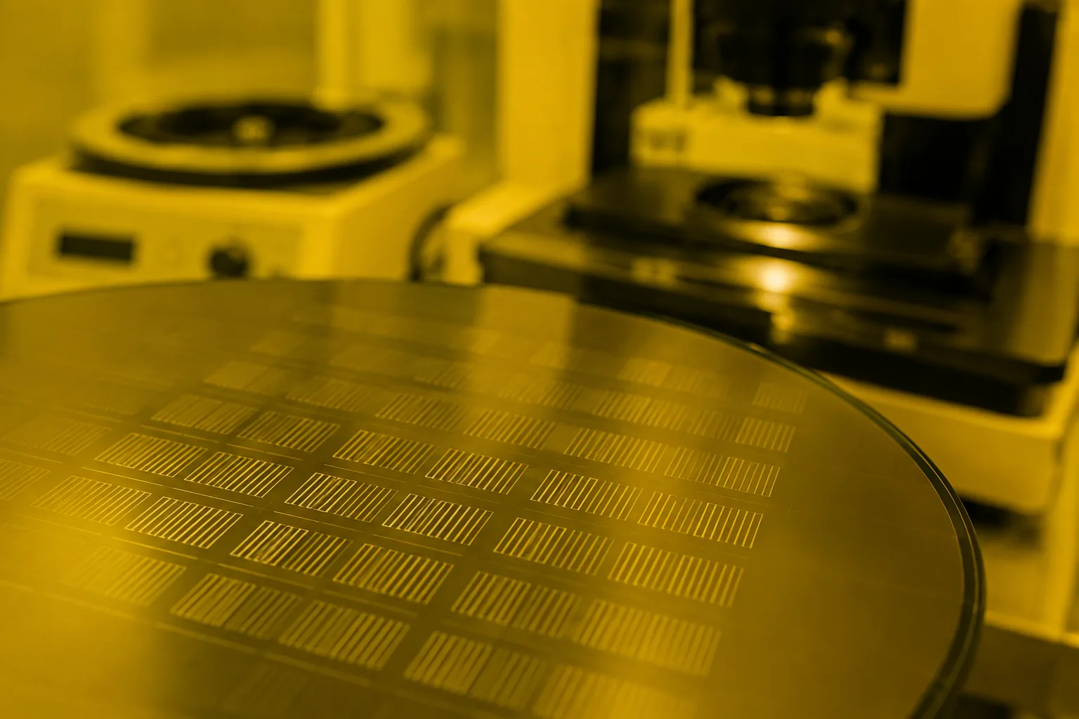
How is film thickness measured after spin coating?
Film thickness is the most fundamental coated-film property, because it sets the achievable resolution, the etch budget, the aspect ratio and the process time for every downstream step. The thickness is determined by the spin-coating process — the spin speed, the resist viscosity, and the solids content — and the measurement confirms that the as-coated film matches the target.
Spin coating is a two-stage process. In the first stage (the coating phase), the resist is dispensed onto the substrate and spread at a relatively low spin speed; the centrifugal force distributes the resist across the wafer while the solvent evaporates and the viscosity rises. In the second stage (the drying phase), the spin speed is ramped higher to accelerate solvent removal and lock in the thickness. The final thickness depends on the viscosity and the spin speed, not on the volume of resist dispensed (assuming enough is dispensed to coat the wafer completely) — the relationship is approximated by the spin-coating equation, where the thickness scales with viscosity to a positive power and with spin speed to a negative power. Typical resist viscosities range from 5 to 35 cSt, and the corresponding thickness range from a few hundred nanometres to over 100 µm for thick-film resists.
The thickness measurement itself uses one of three complementary techniques:
Spectral reflectometry is the workhorse for production and for most laboratory work. The coated wafer is illuminated with white light, the reflected spectrum shows interference fringes from the air-resist and resist-substrate interfaces, and the film thickness is calculated from the fringe spacing and the refractive index. The method is fast, non-contact, and returns the thickness at the measurement point to nanometre-level precision. For a full-wafer uniformity map, the measurement is repeated across a defined site list and the mean, the range and the within-wafer uniformity (typically reported as 3-sigma) are calculated.
Ellipsometry measures the change in polarization of reflected light, and it is the more accurate method for very thin films (below 100 nm) where the reflectometry fringe spacing becomes difficult to resolve. Ellipsometry is the reference for the ultra-thin EUV resist films used in the most advanced nodes.
Profilometry (stylus or optical) measures the step height at a boundary between the coated and the uncoated region (a region where the resist was mechanically removed or never coated). The stylus profilometer (the Dektak-type instrument) drags a diamond stylus across the step and records the vertical displacement; the optical profilometer uses white-light interferometry. Profilometry is the method used when the film is too rough, too transparent or too thick for the optical methods, and it is the method that directly measures the step height rather than inferring the thickness from an optical model.
The reported result for a film-thickness project is the mean thickness, the uniformity (the within-wafer variation), and the comparison to the spin-curve target. A film that is uniformly off-target indicates a spin-parameter or a viscosity problem; a film that is on-target on average but non-uniform indicates a spin-coater or an edge-bead problem. Both are findings the measurement is designed to surface.
How are viscosity and solids content determined?
The viscosity and the solids content are the two liquid-resist properties that most directly determine the coated-film thickness, and they are the two parameters that change when a resist ages, when it is diluted, or when it is contaminated. Both are measured on the liquid resist in the bottle, before coating.
Viscosity is measured under ASTM D2196 (Standard Test Methods for Rheological Properties of Non-Newtonian Materials by Rotational Viscometer) or the equivalent rotational-viscometer methods, and reported in mPa·s or cSt. Photoresist is typically a non-Newtonian fluid — its viscosity depends on the shear rate — and the rotational viscometer measures the viscosity at a defined shear rate and temperature, which the datasheet specifies. The viscosity is the property the spin-curve is built on: a resist with a higher viscosity produces a thicker film at the same spin speed, and a resist whose viscosity has drifted from the datasheet value (through solvent evaporation, through aging, or through contamination) produces a film that does not match the spin-curve target. A viscosity measurement on a suspect lot is the first check when the coated thickness is off-target.
Solids content is measured by the gravimetric method, where a defined mass of the liquid resist is weighed, the solvent is baked off under defined conditions, and the remaining solid mass is weighed again. The solids content is the percentage of the original mass that remains, and it is the property that determines how much polymer is actually deposited on the wafer per unit of coated area. A resist whose solids content has drifted (through solvent loss or through polymer settling) produces a film whose thickness and whose lithographic performance both depart from the datasheet. The gravimetric method is simple and direct, and it is the referee when the spin-curve and the viscosity disagree.
The relationship between the two — the spin-coating equation — is why both matter. Film thickness ≈ k · (viscosity)^a · (spin speed)^(-b), and the viscosity itself is governed by the polymer concentration (the solids content) and the temperature. A lot-to-lot thickness drift that cannot be explained by the spin parameters is almost always a viscosity or a solids-content drift, and the measurement of those two properties is what identifies the root cause. The solids content and the viscosity are the two liquid-resist parameters a Certificate of Analysis reports, and they are the two parameters a lot-acceptance check verifies.
How is the contrast curve and dose-to-clear measured?
The contrast curve and the dose-to-clear are the two lithographic properties that define how the resist responds to exposure, and they are the properties the process engineer optimises the exposure dose against. Both are measured by the open-frame exposure method — a flood exposure at varying doses, with no pattern, followed by development and thickness measurement.
The procedure runs as follows. A wafer is coated with the resist at the target thickness and softbaked. A series of open-frame areas on the wafer are exposed at systematically varying doses — typically using a stepper or a mask aligner with an open-frame mask, or a laser direct writer in flood mode. The wafer is then developed under standard conditions, and the residual film thickness in each exposed field is measured by reflectometry or profilometry. The residual thickness is normalised to the initial film thickness, and the normalised thickness is plotted against the logarithm of the exposure dose.
The resulting curve — the contrast curve — has three regions. At doses below a threshold, the resist does not dissolve in the developer and the full film thickness remains (the unexposed or dark-film region). At doses above a threshold, the resist dissolves completely and the film clears to the substrate (the exposed or clear-film region). Between the two thresholds, the residual thickness decreases with increasing dose (the transition region). Two parameters are extracted:
- Dose-to-clear (E₀) — the minimum dose at which the film fully clears during the standard development. E₀ is the dose the process is normalised against, and it is the parameter the exposure recipe is set to deliver (typically at a multiple of E₀, depending on the feature type and the desired sidewall profile). For a DNQ-Novolac positive resist exposed at i-line (365 nm), E₀ is on the order of tens to hundreds of mJ/cm²; for a chemically amplified resist exposed at DUV or EUV, E₀ is much lower because the chemical amplification multiplies the exposure effect.
- Contrast (γ) — the slope of the contrast curve in the transition region, on the log-dose axis. The contrast is the property that determines the resist's ability to reproduce a sharp pattern edge: a high-contrast resist transitions from full-thickness to cleared over a narrow dose range, producing a steep sidewall; a low-contrast resist transitions over a wide dose range, producing a sloped sidewall. The contrast is the parameter that trade-off against sensitivity (a high-contrast resist typically needs a higher dose) and against resolution (a high-contrast resist typically resolves smaller features).
The contrast curve is the resist's lithographic fingerprint, and it is the measurement that confirms whether a lot behaves like the datasheet or not. A lot whose E₀ has shifted requires an exposure-recipe adjustment; a lot whose contrast has dropped will not resolve the target features regardless of the dose. Both are findings the contrast-curve measurement surfaces, and both are findings the simpler thickness and viscosity measurements cannot detect.
How is dissolution rate characterized?
The dissolution rate is the kinetic property that underlies the contrast curve — the rate at which the exposed resist dissolves in the developer, as a function of the exposure dose. It is measured by the Dissolution Rate Monitor (DRM), an in-situ instrument that measures the resist film thickness in real time during development.
The DRM measurement runs as follows. A wafer is coated, softbaked, and exposed at a defined open-frame dose. The wafer is mounted on the DRM, the developer is introduced, and the instrument measures the film thickness continuously — typically by interferometry, tracking the interference fringes as the film thins — from the moment the developer contacts the resist to the moment the film clears. The time-derivative of the thickness is the instantaneous dissolution rate, and the rate is plotted against the remaining film thickness (or against time). The measurement is repeated at a series of doses, and the resulting rate-vs-dose data is the resist's dissolution kinetics.
Three parameters are extracted from the DRM data:
- The dark-film dissolution rate (R_min) — the rate at which the unexposed resist dissolves in the developer. This is the "dark erosion" that sets the floor on the unexposed-film thickness loss during development, and it is the parameter the developer concentration and the developer temperature are tuned against. A high dark-film rate means the unexposed features lose thickness during development, which narrows the process window.
- The exposed-film dissolution rate (R_max) — the rate at which the fully-exposed resist dissolves. This is the rate that determines the development time, and it is the parameter that the developer normalisation is built on. Typical photoresist dissolution rates range from approximately 100 to 400 nm/s.
- The rate contrast (R_max / R_min) — the ratio of the two. The rate contrast is the kinetic analogue of the contrast-curve γ, and it is the parameter that determines the resist's ability to discriminate between exposed and unexposed regions. A high rate contrast produces sharp pattern edges; a low rate contrast produces diffuse edges.
The DRM is the instrument that resolves the dissolution behaviour that the contrast curve averages over. Where the contrast curve reports the end-state thickness after a fixed development time, the DRM reports the rate at every instant of the development — including the nonlinear dissolution effects (the induction period, the surface-rate suppression, the thickness-dependent rate) that the advanced resist models need to capture. The in-situ DRM characterisation of photoresist dissolution, with typical dissolution rates in the 100–400 nm/s range, is discussed in detail in the lithography-research literature. For EUV resists in particular, where the dissolution behaviour is strongly nonlinear and the film thicknesses are very thin, the DRM is the instrument that characterises the kinetics the contrast curve cannot resolve, and the imec/TEL DRM and the equivalent research-grade instruments are the reference tools for the advanced-node resist development.
How are resolution and sidewall profile qualified?
The resolution and the sidewall profile are the pattern-level properties that the lithographic process is ultimately judged against — the minimum feature size the resist can resolve, and the shape of the features it produces. Both are measured by patterning a defined test mask and inspecting the developed features.
Resolution is qualified by patterning a series of features at progressively smaller dimensions — lines and spaces, contact holes, isolated trenches — and identifying the minimum dimension at which the features resolve cleanly. The resolution is limited by the exposure wavelength (the i-line at 365 nm, the DUV at 248 nm or 193 nm, the EUV at 13.5 nm), by the numerical aperture of the exposure tool, by the resist chemistry, and by the process window. For an i-line DNQ-Novolac resist under optimum conditions, high-resolution thin resists allow feature sizes on the order of 300 nm; for thick-film resists like the SU-8 epoxy, features of 100 µm thickness with aspect ratios above 20 are achievable. The resolution test reports the minimum feature size and the corresponding aspect ratio, and it confirms that the resist resolves the application's target geometry.
Sidewall profile is qualified by cross-sectioning the developed features and measuring the sidewall angle and the profile shape. A positive resist patterned for wet etching typically targets a steep sidewall (near 90°) to minimise the lateral etch bias; a positive resist patterned for lift-off targets an undercut profile (a retrograde sidewall) to ensure the deposited metal does not coat the sidewall; an image-reversal resist can be processed to produce either profile. The sidewall is measured by cleaving the wafer through the feature and imaging the cross-section by Scanning Electron Microscopy (SEM), or by atomic force microscopy (AFM) on a non-cleaved sample. The SEM cross-section also reveals the line-edge roughness (LER) — the stochastic variation of the feature edge position — which is the parameter that limits the CD control at the advanced nodes.
The resolution and the sidewall are the properties that the open-frame contrast-curve measurement cannot predict alone, because they depend on the aerial image (the spatial distribution of the exposure dose), the resist's response to that aerial image, and the development kinetics in the presence of the pattern geometry. A complete lithographic characterization includes the open-frame contrast curve (the resist's intrinsic response) and the patterned resolution and sidewall (the resist's response in the actual application geometry), because the two together describe the resist's behaviour from the intrinsic to the applied.
How is residual photoresist detected after stripping?
The post-strip residual-resist detection is the cleanliness check that confirms the photoresist has been completely removed after patterning, before the wafer moves to the next process step. As semiconductor patterning has shrunk below 10 nm, the residual-contamination problem has become more severe, because the same absolute residue that was tolerable at a larger node is a larger fraction of the feature dimension at a smaller node, and because the higher pattern density increases the residue-holding surface area.
The detection runs by two complementary methods:
Optical inspection is the routine method. The stripped wafer is inspected under a microscope — brightfield, darkfield, or fluorescence. Fluorescence microscopy has the advantage for this application, because the residual photoresist is organic and the organic material fluoresces under UV excitation, where the bare silicon substrate does not. The contrast between the fluorescing residue and the non-fluorescing substrate makes even small amounts of residue visible against the background, where brightfield or darkfield inspection would miss it. The inspection reports the location, the size and the density of the residual-resist defects.
Full-wafer fluorescence scanning is the production-scale method. The stripped wafer is scanned by a defect-inspection tool (the Surfscan SP2 and equivalent) equipped with a UV source and a fluorescence-detection channel. The tool generates a full-wafer fluorescence map — a "SURFimage" — that shows the regions of the wafer where residual photoresist is present. The method takes advantage of the same fluorescence property as the microscopy, but at the full-wafer scale and with the sensitivity to detect residue that the current metrology and analytical methods (the ones that report only the particle count) do not resolve.
The residual-resist detection is the closing check of the photoresist lifecycle. A wafer that passes the lithographic patterning and the development can still fail the post-strip cleanliness, and the residue that the standard particle-count inspection misses is caught by the fluorescence method. This is the measurement that confirms the photoresist removal process (the ash and the clean) has done its job, and it is the measurement that closes the loop from the liquid resist through the coated film, the exposed pattern, and the stripped wafer.
FAQ
Which standard should my photoresist be tested to?
Photoresist does not have a single dedicated international product standard. The framework is method-driven: viscosity under ASTM D2196, solids content by the gravimetric method, film thickness by spectral reflectometry or ellipsometry, dissolution rate by DRM, and the lithographic properties by the open-frame and patterned-exposure methods the vendor CoA references. A common error is to cite SEMI C35 for photoresist — SEMI C35 is the nitric acid specification, not a photoresist standard. We confirm the property set against the application before quoting.
What is the dose-to-clear, and why does it matter?
E₀ is the minimum open-frame exposure dose at which the resist film fully clears during standard development. It is the parameter the exposure recipe is set against (typically at a multiple of E₀), and it is the parameter that shifts when a lot ages, when the process temperature drifts, or when the resist chemistry changes. A lot whose E₀ has shifted can be corrected by a recipe adjustment; a lot whose contrast has dropped cannot, and the two are distinguished by the contrast-curve measurement.
Can you measure the spin curve for our resist on our spin coater?
Yes. The spin curve — film thickness as a function of spin speed, at a defined viscosity and temperature — is the empirical relationship the process recipe is built on. We coat the resist on your substrate (or an equivalent) at a series of spin speeds, measure the thickness at each speed by reflectometry, and fit the spin-coating equation. The spin curve confirms the resist's thickness range on the specified equipment, and it is the measurement that translates the liquid-resist viscosity into the coated-film thickness the application requires.
What sample do you need for a contrast-curve measurement?
Coated wafers (or coated substrate pieces) at the target film thickness, softbaked under the standard condition. We perform the open-frame exposure series, the development, and the residual-thickness measurement on our equipment. For a project that includes the dissolution-rate characterisation, additional coated samples are exposed at defined doses for the DRM measurement. We confirm the substrate, the thickness and the softbake condition before testing.
Can you detect residual photoresist on wafers after ash and clean?
Yes. We inspect by optical microscopy (brightfield, darkfield, fluorescence) for the routine check, and we perform full-wafer fluorescence scanning for the production-scale check. The fluorescence method exploits the organic nature of the residual photoresist, which fluoresces under UV excitation where the bare substrate does not, and it resolves residue that the particle-count inspection misses. This is the measurement that confirms the post-strip cleanliness.
Our photoresist testing service
Our laboratory provides photoresist testing across the full property set — the liquid-resist properties (viscosity, solids content, particle count), the coated-film properties (thickness, uniformity, refractive index), the lithographic properties (contrast curve, E₀, dissolution rate, resolution, sidewall profile), the process-compatibility properties (thermal flow, etch resistance, developer and stripper compatibility), and the post-strip cleanliness (residual-resist detection by fluorescence). Each project begins with a scoping step that confirms the application (wet etch, dry etch, lift-off, electroplating, thick-film structure, grayscale 3D, EUV) and maps the property set to the corresponding methods, so the report you receive answers the question your process engineer or your customer will actually ask.
We measure viscosity under ASTM D2196 and solids content by the gravimetric method on the liquid resist; film thickness by spectral reflectometry, ellipsometry and profilometry on the coated wafer; the contrast curve and E₀ by open-frame exposure with residual-thickness measurement; the dissolution rate by the in-situ DRM; resolution and sidewall profile by patterned exposure with SEM cross-sectioning; and residual-resist by optical inspection and full-wafer fluorescence scanning. Reports are issued with the method, the measured value, the datasheet or control value, and the conformity conclusion explicitly stated, with the contrast curves, the DRM rate plots and the SEM images included where the result depends on them, in a format suitable for lot acceptance, process-window qualification, resist-selection comparison or failure investigation.
To start a project, send us the resist grade and the vendor datasheet, the application and the target film thickness, the exposure wavelength and tool, and whether the project is lot acceptance, process-window qualification, resist selection, or failure investigation. We will return a project scope, sample requirement, schedule and quotation, and begin testing on your confirmation.