Scanning Electron Microscopy (SEM) is one of the most versatile and widely used tools in modern analytical laboratories. Unlike optical microscopes that rely on visible light, SEM uses a finely focused beam of high-energy electrons that scans across the sample surface in a raster pattern. The interactions between the electron beam and the specimen produce multiple signals—secondary electrons, backscattered electrons, characteristic X-rays, and more—which are captured by dedicated detectors to generate highly detailed images and elemental data. With magnifications routinely exceeding 100,000× and resolution reaching the nanoscale, SEM provides a level of surface detail that is unattainable with traditional microscopy.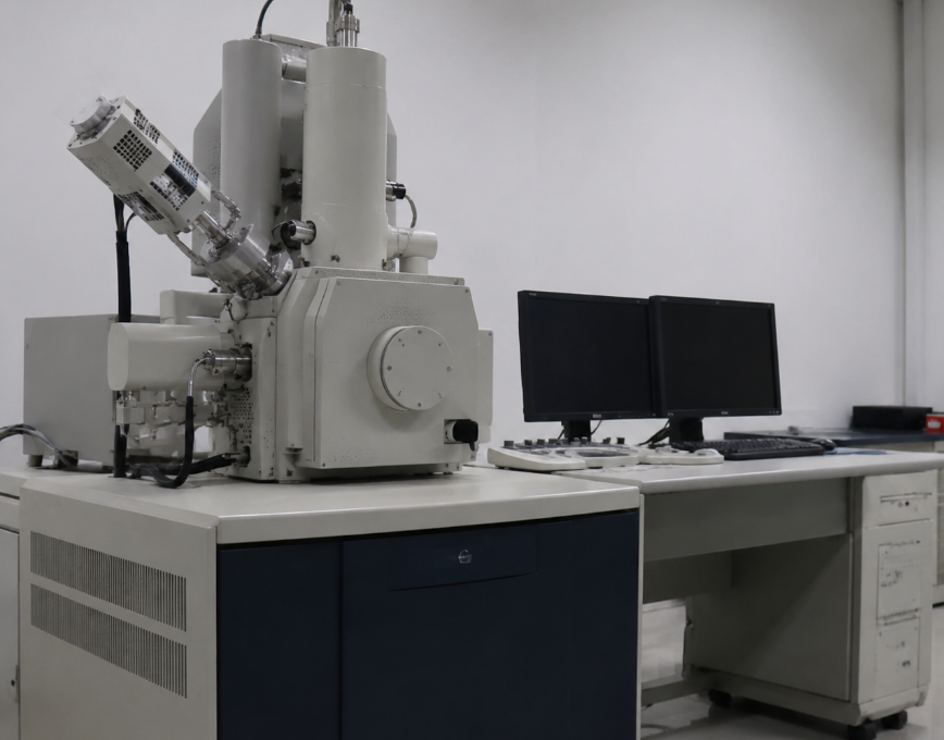
The core strength of SEM lies in its dual capability: topographical imaging and compositional analysis. Secondary electron (SE) imaging delivers remarkable three-dimensional surface detail, making it ideal for studying fracture surfaces, particulate morphology, and microstructural features. Backscattered electron (BSE) imaging, on the other hand, provides atomic number contrast, revealing variations in chemical composition across the sample. When equipped with an Energy Dispersive X-ray Spectrometer (EDS), the SEM can identify and map the elemental constituents of microscopic regions, delivering both qualitative and semi-quantitative information in real time.
The applications of SEM-EDS span virtually every scientific and industrial sector. In materials science and metallurgy, it is used to examine grain boundaries, inclusions, coatings, and weld integrity. failure analysis engineers depend on SEM to identify the root causes of component fractures, corrosion pits, and contamination. In the semiconductor and electronics industries, SEM performs critical dimension measurements, defect inspection, and cross-sectional analysis of integrated circuits. Biomedical and life sciences laboratories use SEM to visualize cell morphology, tissue structures, biomaterials, and the interfaces between implants and biological tissues. Forensic science relies on SEM-EDS to analyze gunshot residue, paint fragments, and trace evidence. Geology and environmental sciences benefit from its ability to characterize mineral phases, airborne particulates, and soil contaminants.
At Beijing ZKGX Research Institute of Science and Technology, we operate state-of-the-art field-emission SEM systems integrated with advanced EDS detectors, enabling nanoscale resolution and rapid elemental mapping. Our ISO 17025 accredited laboratory delivers comprehensive SEM services, including high-resolution imaging, particle size and morphology analysis, coating thickness measurement, failure analysis, and contamination identification. Supported by a team of experienced scientists, we provide tailored analytical solutions, rigorous data quality, and detailed technical reports that meet the stringent demands of research, product development, and regulatory compliance.