What Does "Transistor Testing" Mean in a Laboratory?
A transistor is a three-terminal semiconductor device — bipolar junction transistor (BJT, NPN/PNP) or field-effect transistor (FET: MOSFET, JFET, IGBT) — that switches or amplifies current, and it is the building block of every active electronic circuit. "Transistor testing" in a laboratory is the characterisation, qualification and reliability verification of a discrete transistor against its datasheet and the applicable semiconductor-device standard. It is governed internationally by the IEC 60747-7 (bipolar transistors) and IEC 60747-8 (field-effect transistors) standards; in China by GB/T 4587-2023《半导体器件 分立器件 第7部分:双极型晶体管》(replacing GB/T 4587-1994, equivalent adoption of IEC 60747-7) and GB/T 4586-1994《分立器件 第8部分:场效应晶体管》(≡ IEC 747-8:1984); and for high-reliability by MIL-STD-750 (discrete-semiconductor test methods). It is distinct from the multimeter pass/fail "transistor test" that dominates the consumer SERP — that is field troubleshooting, which detects only dead-short or dead-open junctions. A laboratory transistor test measures the electrical parameters (gain, leakage, breakdown, switching) on a curve tracer / parameter analyser, quantitatively against the datasheet — the difference between "is it completely dead?" and "does it meet spec?".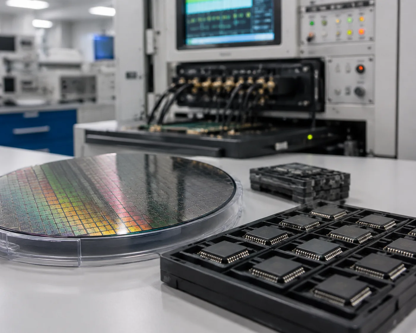
Why a Laboratory Test Is Not a Multimeter Pass/Fail
The competitor material on the SERP is almost entirely how to test a transistor with a multimeter in diode mode — apply the probes to base-emitter and base-collector, expect ~0.6–0.9 V forward and "OL" reverse, declare the part good or bad. That test answers only one question: is the transistor shorted or open? It does not measure:
- DC current gain (h_FE / h21) — the amplification factor; a transistor can pass the multimeter diode test yet have h_FE far below datasheet.
- Leakage currents (I_CBO, I_CEO, I_EBO) — the unwanted reverse currents that flag degradation; a high-leakage part passes the multimeter but fails in circuit.
- Breakdown voltages (BV_CBO, BV_CEO, BV_EBO) — the reverse-voltage limits; measured at a specified leakage-current threshold, not by diode-mode probing.
- Switching times (t_on, t_off, t_d, t_r, t_s, t_f) — the speed parameters; not measurable by any multimeter.
- The output characteristic family — the I_C vs V_CE curves at stepped base currents, the true characterisation of the device.
A multimeter test that "passes" a transistor therefore proves only that it is not completely dead; a laboratory characterisation verifies that it meets its datasheet — and the gap between these two is exactly where field "good" parts fail in service.
What Are the Core BJT Tests?
For a bipolar transistor the full parameter characterisation per IEC 60747-7 / GB/T 4587-2023 covers four families of parameters:
1. Gain. DC current gain h_FE (also h21, β) — the ratio of collector current to base current at a specified V_CE and I_C; measured with a parameter analyser or a multimeter with an h_FE socket, and checked against the datasheet's h_FE classification (e.g. the "h21 grouping" bands). Gain varies with collector current and temperature, so the test specifies both.
2. Leakage. The three reverse leakage currents — I_CBO (collector-base, emitter open), I_CEO (collector-emitter, base open) and I_EBO (emitter-base, collector open) — measured at the rated reverse voltage; a high leakage indicates junction degradation and is a leading early-failure indicator.
3. Breakdown. The three breakdown voltages — BV_CBO, BV_CEO, BV_EBO — measured as the reverse voltage at which the leakage reaches a specified current threshold; these are the absolute-maximum limits the circuit designer must respect. Breakdown testing is destructive-capable, so the compliance current is set to protect the device.
4. Switching. The switching times t_on, t_off, t_d (delay), t_r (rise), t_s (storage), t_f (fall) at specified drive and load — the speed characterisation for switching applications; measured with a pulsed drive and a fast oscilloscope.
How Is the Characterisation Performed — Curve Tracer / Parameter Analyser?
The instrument that defines transistor laboratory testing is the curve tracer (or transistor parameter analyser, e.g. Tektronix 370A / 371A, Keysight B1500, Keithley 4200). It forces a swept voltage (or current) while measuring the response, stepping a second parameter (base current, gate voltage) to build a family of curves:
- Output characteristic family — I_C vs V_CE, stepped in I_B, the canonical BJT characterisation; shows the saturation, active and breakdown regions.
- Input characteristic — I_B vs V_BE at fixed V_CE; the diode-like base-emitter curve.
- Transfer characteristic — I_C vs I_B at fixed V_CE; the gain (slope).
- FET characteristics — I_D vs V_DS stepped in V_GS (output), I_D vs V_GS at fixed V_DS (transfer, gives g_m and V_th).
For MOSFETs the gate is capacitively driven, so the test sequence includes a gate-charge (Q_g) measurement and the threshold-voltage (V_th) extraction; for JFETs the pinch-off voltage (V_GS(off)) is the key parameter. Modern parameter analysers integrate the SMU (source-measure unit) per terminal, with sub-picoamp leakage resolution and pulse-measurement capability to avoid self-heating — the IEC 60747 / GB/T 4587 methods recommend pulse measurement to suppress junction-temperature rise during the test.
What Are the Reliability and Qualification Tests?
A discrete transistor carries the same reliability burden as any semiconductor device, governed for high-rel by MIL-STD-750 (the discrete-semiconductor counterpart of MIL-STD-883 for microcircuits) and GJB 128 in China:
- Burn-in / high-temperature reverse bias (HTRB) — operates the device at elevated temperature and reverse bias to weed out infant-mortality failures.
- Temperature cycling / thermal shock — verifies the die-attach, wire-bond and package survive the declared temperature range.
- Steady-state and intermittent operating life — accelerates aging to predict service life.
- ESD sensitivity — Human-Body-Model (HBM) and Machine-Model (MM) classification; FETs (especially MOSFETs and IGBTs) are notoriously ESD-sensitive through the gate oxide, so the ESD test is mandatory.
- dV/dt immunity (power MOSFETs) — the rate-of-voltage-change at which a power MOSFET false-triggers through the Miller capacitance; a critical parameter for switching-power applications.
- Safe Operating Area (SOA) / avalanche — verifies the device survives the declared V_DS × I_D stress and the avalanche-energy rating.
How Do BJT, MOSFET, JFET and IGBT Tests Differ?
The four transistor families share the three-terminal structure but differ in what must be measured:
| Family | Key DC parameters | Distinctive tests |
|---|---|---|
| BJT (NPN/PNP) | h_FE, I_CBO/I_CEO/I_EBO, BV_CBO/BV_CEO/BV_EBO, V_CE(sat) | Diode-mode B-E / B-C forward ~0.6–0.9 V; h_FE socket |
| MOSFET | V_th, R_DS(on), I_DSS, g_m, Q_g | Gate-charge; dV/dt immunity; SOA/avalanche; ESD (gate oxide) |
| JFET | I_DSS, V_GS(off), g_m | Pinch-off; low drain-source resistance (channel "on") |
| IGBT | V_CE(on), V_GE(th), I_CES, switching times | Gate-emitter threshold; tail-current at turn-off; SOA |
The MOSFET and IGBT gate is an insulated capacitive input, so the gate must be charged/discharged to switch — and the ESD and dV/dt sensitivities that follow have no BJT equivalent.
What Belongs on the Report?
A compliant transistor test report states the device type (BJT/FET family, NPN/PNP, package), the standard (GB/T 4587-2023 / IEC 60747-7 BJT; GB/T 4586 / IEC 60747-8 FET; MIL-STD-750 / GJB 128 high-rel), the parameter family (gain / leakage / breakdown / switching / reliability), the test conditions (I_C, V_CE, temperature, pulse vs DC), and the result against the datasheet limit. For reliability it reports the burn-in/temperature-cycling result and the achieved life; for ESD it reports the HBM/MM classification. Conflating a multimeter diode-mode pass with a parameter characterisation is the cardinal error.
For the related discrete-semiconductor service within the broader component framework, see Electronic Component Testing; for integrated-circuit testing, integrated circuit testing.
FAQ
What is the difference between a multimeter transistor test and a laboratory transistor test?
A multimeter diode-mode test only checks that the base-emitter and base-collector junctions are not shorted or open (~0.6–0.9 V forward, "OL" reverse) — it detects a completely dead part. A laboratory test characterises the device on a curve tracer / parameter analyser — measuring h_FE, leakage, breakdown, switching, output-characteristic family — quantitatively against the datasheet. The gap is where field "good" parts fail in service.
What is h_FE (h21, β) and how is it measured?
h_FE is the DC current gain — the ratio of collector current to base current at a specified V_CE and I_C. It is measured with a parameter analyser or a multimeter with an h_FE socket, and verified against the datasheet's gain classification. Gain varies with collector current and temperature, so the test specifies both; a low h_FE is a common out-of-spec failure that a multimeter diode test will not catch.
Why are MOSFETs more ESD-sensitive than BJTs?
Because the MOSFET gate is a thin silicon-oxide insulator; an ESD event punctures the oxide and destroys the gate, whereas a BJT gate (the base) is a forward-biased junction that clamps. This is why MOSFETs, JFETs and IGBTs require ESD-controlled handling and ESD-sensitivity classification (HBM/MM) as part of their test program — a test that has no BJT equivalent.
Which standards govern transistor testing?
Bipolar transistors: IEC 60747-7 / GB/T 4587-2023 (replacing GB/T 4587-1994). Field-effect transistors: IEC 60747-8:2010 / GB/T 4586-1994 (≡ IEC 747-8:1984). High-reliability: MIL-STD-750 (the discrete-semiconductor counterpart of MIL-STD-883) and GJB 128 in China. The IEC 60747 / GB methods recommend pulse measurement to suppress self-heating.
What are the four basic transistor tests in practical troubleshooting?
Gain (h_FE), leakage (I_CBO/I_CEO/I_EBO), breakdown (BV_CBO/BV_CEO/BV_EBO), and switching time (t_on/t_off and the components t_d, t_r, t_s, t_f). For maintenance a check of two or three of these is usually sufficient to decide replace-or-keep; for qualification the full parameter set plus reliability is required.
Our Testing Capabilities
As an ISO/IEC 17025-accredited third-party laboratory, Beijing ZKGX Research provides transistor testing across the four families (BJT, MOSFET, JFET, IGBT) and both commercial and high-reliability frameworks:
- BJT characterisation — h_FE / h21, I_CBO/I_CEO/I_EBO leakage, BV_CBO/BV_CEO/BV_EBO breakdown, V_CE(sat), output/input/transfer characteristic families, to GB/T 4587-2023 / IEC 60747-7.
- FET characterisation — V_th, R_DS(on) (MOSFET), I_DSS, V_GS(off) (JFET), g_m, Q_g (MOSFET), output and transfer curves, to GB/T 4586 / IEC 60747-8:2010.
- IGBT — V_CE(on), V_GE(th), I_CES, switching times (incl. tail-current), SOA.
- Switching / dynamic — t_on, t_off, t_d, t_r, t_s, t_f at specified drive and load, by pulsed drive + fast oscilloscope.
- Reliability / qualification — burn-in / HTRB, temperature cycling, steady-state and intermittent operating life, to MIL-STD-750 / GJB 128 and the commercial GB/T framework.
- ESD and dV/dt — HBM/MM classification (mandatory for MOSFET/IGBT gate oxide), dV/dt immunity and avalanche/SOA for power MOSFETs.
Sample types include small-signal BJT, power BJT, low-voltage and power MOSFET, JFET, IGBT, RF transistor, in through-hole and surface-mount packages. If you have a specific device family, standard (GB/T 4587 / IEC 60747-7 / GB/T 4586 / IEC 60747-8 / MIL-STD-750 / GJB 128), parameter requirement (h_FE / leakage / breakdown / switching / reliability), or application (amplification / switching / power / RF / automotive), contact the laboratory to confirm the exact test set and reporting format before testing.