What Does "Integrated Circuit (IC) Testing" Mean in a Laboratory?
An integrated circuit (IC) is a miniature semiconductor device housing thousands to billions of transistors and other components on a single chip of silicon — from simple op-amps and memory to the most complex system-on-chip (SoC) and 3D-stacked processor. "Integrated circuit testing" is the verification of an IC's functional correctness, electrical performance, and reliability through a coordinated programme of tests applied at defined points in the manufacturing and product lifecycle. It is governed internationally by JEDEC (commercial) and MIL-STD-883 / MIL-PRF-38535 (high-reliability), in China by the GB/T 17574 / GB/T 16464 national framework (digital IC, identical adoption of IEC 60748), the SJ/T industry test-method standards for specific circuit families, and for high-rel by GJB 597B-2012 (≡ MIL-PRF-38535) and GJB 548C-2021 (≡ MIL-STD-883). It is distinct from the broader electronic-component testing (which covers passives, discretes and electromechanicals as well) and from optoelectronic-device testing (LED/LD/PD/sensor) — IC testing concerns only the integrated-circuit chip, both bare die and packaged, and its unique DFT (design-for-test) infrastructure.
Why IC Testing Spans Two Levels — Wafer and Package
The defining structural fact of IC testing is that it happens at two physical levels, and the test content differs at each: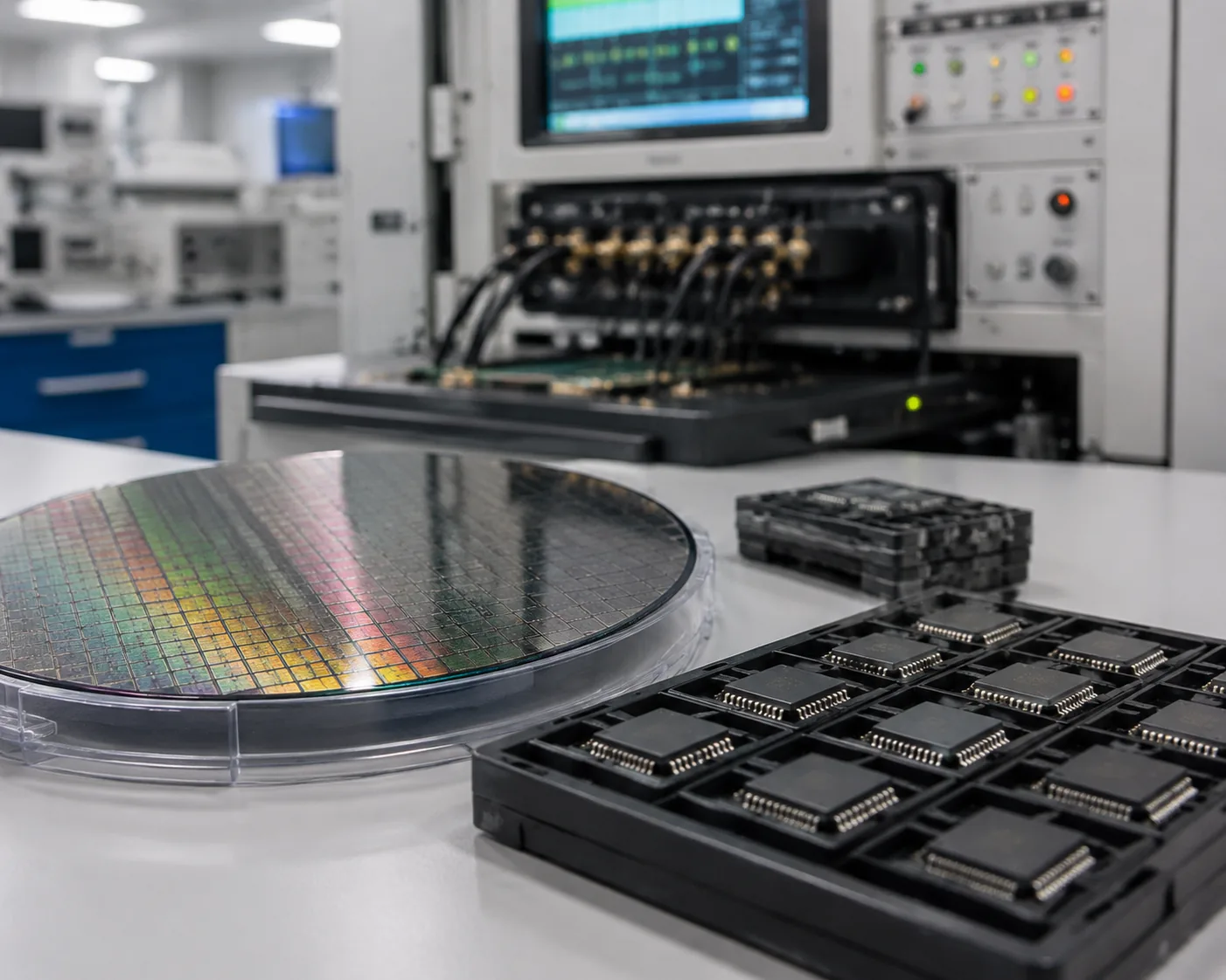
- Wafer test (chip-probe / CP test) — performed on the bare die while still on the wafer, before singulation and packaging, using automatic test equipment (ATE) with a probe card (needle-like probes) that contact the wafer bond pads. The purpose is to identify defective dies early, before the cost of packaging is added — critical for new process nodes where it provides yield feedback to the foundry — and to enable wafer-level binning (sorting dies into performance/feature bins for differential pricing). Test content is typically simple functional + parametric, to detect gross defects at speed.
- Package test (final test / FT) — performed on the packaged IC, after the die is singulated, bonded and sealed in its package. The package adds physical protection, electrical isolation, heat dissipation and signal distribution, but it can also introduce new defects (bond wire opens/shorts, solder bridge, cracked die). Package test re-verifies the IC electrically and adds functional, signal-integrity, power, noise and thermal checks under realistic conditions. For mature processes with proven yield, wafer testing is sometimes optional and only package testing is performed.
The two levels are complementary, not alternatives: a die that passes CP can fail FT (packaging-induced), and the cost-benefit of CP vs FT depends on process maturity and packaging cost.
What Are the Eight Test Categories?
Within and across the two levels, eight test categories cover the full IC-test programme:
- Wafer test (CP) — early gross-defect screen on bare die (above).
- Final / package test (FT) — full electrical + functional + parametric on the packaged IC.
- Reliability testing — accelerated aging (burn-in), temperature cycling, thermal shock, humidity, life test to predict long-term reliability per GJB 548C / MIL-STD-883 Method 1005/1010 and GB/T 33768-type standards.
- Parametric testing — DC and AC parametric measurements (V_OH/V_OL, I_CC, propagation delay, setup/hold) against datasheet limits.
- In-circuit testing (ICT) — verifies the IC after it is assembled onto a PCB, using a bed-of-nails fixture with spring-loaded pogo pins; detects manufacturing defects (wrong component, open/short, orientation) rather than IC design faults.
- Boundary-scan (JTAG / IEEE 1149.1) — uses the JTAG test-access port and boundary-scan register to test interconnections and on-chip logic without physical probe access; essential for high-pin-count BGA packages where bed-of-nails cannot reach.
- Memory testing — March algorithms and bit-map diagnostics detect stuck-at, coupling and address-decoder faults in embedded and standalone memory.
- Yield analysis — analyses the % of good dies per wafer to identify and address manufacturing-process issues; complements CP test data with failure-analysis feedback.
These methods are typically combined — a production IC is wafer-tested, package-tested, reliability-screened, and shipped with a yield-analysis record.
What Is Design-for-Test (DFT), and Why Is It the Modern IC-Test Foundation?
As IC complexity scaled to billions of transistors, testing from the external pins alone became intractable, so design-for-test (DFT) structures are built into the chip itself. The four pillars:
- Scan-based structural test — internal flip-flops are chained into shift registers (scan chains) during test mode, giving the ATE direct controllability and observability of internal nodes. Automatic test pattern generation (ATPG) algorithmically creates the input vectors that detect stuck-at and transition faults. Structural scan coverage (target ≥ 95–99 %) is the dominant production-fault-detection metric.
- Built-in self-test (BIST) — on-chip pattern generators (LFSR) and response compressors (MISR) generate and analyse test patterns internally, returning only a pass/fail signature — critical for embedded memory (memory BIST) and logic (logic BIST), where it cuts ATE test-data volume and time.
- Test compression — coding, scan-chain restructuring and compaction schemes reduce the test-data volume and ATE bandwidth needed for ultra-large-scale ICs, with substantial reductions in test time and equipment cost.
- IEEE 1500 (embedded-core test) — for SoCs that embed reusable IP cores, IEEE Std 1500 (2005) wraps each core with a standard test wrapper and defines the test access mechanism (TAM) and core test language (CTL) that let each core be controlled and observed from the SoC pins regardless of the IP vendor. Without IEEE 1500, embedded-core testing of a multi-vendor SoC would be impossible.
Energy-efficient testing is now part of DFT: because at-speed scan testing dissipates far more power than normal operation (causing overheating, yield loss, even damage), low-power ATPG, scan-segmentation, gated clocks and test-data compression are used to keep test power within the chip's thermal budget.
How Do 3D-IC and SoC Testing Differ From Planar IC Testing?
Two emerging architectures drive new test methods beyond the planar-IC framework:
3D stacked ICs (TSV-based) — multiple active layers bonded with through-silicon vias (TSVs). Testing follows a four-stage sequence: pre-bond die test (KGD — known-good-die, before stacking), mid-bond partial-stack test (after some layers are bonded), post-bond full-stack test (verifies the TSVs and the assembled stack, where TSV defects — microvoids, pinholes, seed-layer residue, misalignment — appear), and final packaged test. The new fault models are TSV-interconnect defects and 3D-process-induced defects (wafer-thinning damage, thermal-stress cracks), which standard 2D tests do not catch. Limited edge-pin count makes per-layer observability hard, which is why KGD pre-bond testing is so important.
System-on-Chip (SoC) with embedded cores — testing is governed by IEEE 1500 (above), where each embedded IP core needs its own wrapper, TAM and CTL description. The challenge is matching the core's data width to the SoC's pin count, and reusing each core's test patterns at the SoC level without re-developing them — exactly the problem IEEE 1500 was written to solve.
How Do the Military-Qualification Levels Apply to ICs?
For high-reliability ICs (aerospace, defence, space, automotive-safety), the GJB 597B-2012 / MIL-PRF-38535 qualification defines quality-assurance levels of increasing screening rigour:
| Level (GJB 597B / MIL-PRF-38535) | Screening rigour |
|---|---|
| B / Class B | High-reliability — full screening (100 % burn-in, PIND, hermeticity), the workhorse hi-rel level |
| BG / Class Q | Higher — additional screening for critical applications |
| S / Class S / Class V | Space / radiation-hardened — the highest, most extensive testing and environmental screening |
The test methods themselves are in GJB 548C-2021 / MIL-STD-883 (Method 1005 burn-in, 1010 temperature cycling, 1009 solderability, PIND, fine/gross leak, DPA), applied at the screening level declared. A commercial-grade IC tested only to GB/T 17574 / SJ/T does not carry a GJB 597B level — the level is what the high-rel customer specifies.
What Are the Commercial GB/T / SJ/T Standards?
For non-military commercial ICs, the Chinese framework is:
- GB/T 16464-1996 / GB/T 17574-1998 / GB/T 17573-1998 — the 总则 (general) framework for IC and digital-IC testing, identical adoption of IEC 60748-1 / 60748-2 / 60747-1.
- Circuit-family SJ/T test methods — SJ/T 10741-2000 (CMOS), SJ/T 10804-2000 (level shifter), SJ/T 10805-2018 (voltage comparator), SJ/T 11702-2018 (serial peripheral interface), SJ/T 11706-2018 (FPGA), SJ/T 11875-2022 (automotive stress), SJ/T 10427.1-1993 (audio), SJ/T 12036-2025 (IC test metrics).
- GB/T device-specific — GB/T 4377 (voltage regulator), GB/T 14028 (analogue switch), GB/T 42975-2023 (driver), GB/T 42838-2023 (Hall), GB/T 6798 (comparator), GB/T 15876 (plastic QFP leadframe), GB/T 35000-2018 (EMI 1 kHz–1 GHz), GB/T 42974-2023 (FLASH).
The GB/T / SJ-T framework and the GJB / MIL-STD framework use related but separate test sequences and the qualification levels (B/BG/S) apply only to the military framework.
What Belongs on the Report?
A compliant IC test report states the IC type, the test level (wafer / package / in-circuit), the test categories covered (functional, parametric, reliability, DFT scan coverage), the standard and method (e.g. SJ/T 10741 CMOS, GJB 548C Method 1005 burn-in, IEEE 1149.1 boundary scan, IEEE 1500 embedded core), the test conditions, and the result against the datasheet/acceptance criterion. For high-reliability qualification it states the GJB 597B / MIL-PRF-38535 level (B / BG / S) claimed and verified. For 3D-IC it states the test stage (pre-bond / mid-bond / post-bond / packaged). Conflating levels — e.g. reporting a CP result as a final-test result — is a common error.
For the broader electronic-component counterpart, see Electronic Component Testing; for the optoelectronic-device subset, Optoelectronic Device Testing; for failure investigation of a failed IC, electronic component failure analysis.
FAQ
What is the difference between wafer test and package test?
Wafer test (CP) is performed on the bare die on the wafer before packaging, using ATE + probe card, to screen out defective dies early and enable wafer-level binning. Package test (FT) is performed on the packaged IC to verify electrical performance, functionality, signal integrity and thermal behaviour under realistic conditions, and to catch packaging-induced defects. For mature processes, CP may be optional; for new nodes, CP is essential for yield feedback.
What is design-for-test (DFT), and why is it needed?
DFT is test infrastructure built into the IC — scan chains, BIST, test compression, IEEE 1149.1 / IEEE 1500 wrappers — that gives the ATE controllability and observability of internal nodes that the external pins alone cannot provide on a billion-transistor chip. Without DFT, an IC of modern complexity could not be tested in any reasonable time or at any reasonable fault coverage.
What are the GJB 597B / MIL-PRF-38535 qualification levels?
Three levels of increasing screening: B / Class B (high-reliability, full 100 % screening — the workhorse hi-rel level), BG / Class Q (higher, additional screening for critical applications), S / Class S / Class V (space / radiation-hardened, the highest, most extensive testing). The level is what the high-rel customer specifies on the purchase order; a commercial-grade IC tested only to GB/T 17574 does not carry a GJB 597B level.
How is 3D-IC testing different from planar IC testing?
3D ICs (TSV-stacked) add a four-stage test sequence — pre-bond KGD, mid-bond partial stack, post-bond full stack, packaged — and new fault models for TSV interconnects (microvoids, pinholes, misalignment) and 3D-process-induced defects (wafer-thinning damage, thermal-stress cracks) that standard 2D tests do not catch. Limited edge-pin count makes per-layer observability hard, so known-good-die pre-bond testing is essential.
Which Chinese standards govern IC testing?
The general framework is GB/T 16464 / GB/T 17574 / GB/T 17573 (≡ IEC 60748 / 60747-1). Circuit-family methods are SJ/T 10741 (CMOS), SJ/T 10805 (comparator), SJ/T 11702 (SPI), SJ/T 11706 (FPGA), SJ/T 11875 (automotive), plus device-specific GB/T standards. High-rel uses GJB 597B-2012 (≡ MIL-PRF-38535) and GJB 548C-2021 (≡ MIL-STD-883). TC599 (全国集成电路标准化技术委员会) is the responsible body.
Our Testing Capabilities
As an ISO/IEC 17025-accredited third-party laboratory, Beijing ZKGX Research provides integrated circuit testing across the two levels, the eight categories and both the commercial and high-reliability frameworks:
- Wafer test (CP) — ATE + probe-card gross-defect and parametric screening of bare die, with wafer-level binning and yield-analysis reporting.
- Package test (FT) — full electrical, functional, parametric, signal-integrity, power and thermal verification of packaged ICs, including memory-test (March algorithms) and JTAG / IEEE 1149.1 boundary scan.
- DFT-aware structural test — scan-chain + ATPG coverage (target ≥ 95–99 %), logic/memory BIST, test compression, and IEEE 1500 embedded-core test on SoCs.
- Reliability / qualification — burn-in (GJB 548C Method 1005), temperature cycling, thermal shock, humidity, steady-state and intermittent operating life, to GJB 548C / MIL-STD-883 and GB/T 33768.
- 3D-IC test — pre-bond KGD, mid-bond, post-bond TSV verification, and packaged 3D-stack test.
- High-rel qualification — GJB 597B-2012 (B / BG / S levels) with the full GJB 548C screening sequence; upscreening of commercial ICs to hi-rel.
- Commercial-framework testing — GB/T 17574 / GB/T 16464 general, plus circuit-family SJ/T methods (CMOS, comparator, SPI, FPGA, driver, Hall, FLASH, automotive stress).
Sample types include bare die, packaged digital/analogue/mixed-signal ICs, memory, microprocessors, SoCs, FPGAs, and 3D-stacked ICs. If you have a specific IC type, test level (wafer/package/in-circuit), qualification target (GB/T commercial / GJB 597B B-BG-S / MIL-PRF-38535 / JEDEC), or DFT requirement (scan / BIST / IEEE 1500), contact the laboratory to confirm the exact test set and reporting format before testing.