What Does "Optoelectronic Device Testing" Mean in a Laboratory?
Optoelectronic (photonic) devices are semiconductor components that convert between electrical and optical signals — the building blocks of every LED, laser diode (LD), photodiode (PD), image sensor (CCD/CMOS), optical modulator, photonic integrated circuit (PIC), and fibre-optic transceiver. "Optoelectronic device testing" in a laboratory is therefore the electrical-and-optical characterisation, qualification and reliability verification of these components against their datasheet and application specifications, before they go into a system. It is governed internationally by the IEC 60747-5 family (Semiconductor devices — Optoelectronic devices) and by device-specific standards (e.g. IEC 60747-5-6 LEDs, -5-7 photodiodes, -5-5 optocouplers); in China by the GB/T 15651 national series (identical adoption of IEC 60747-5) plus the SJ/T 11394-2009 industry LED test method and the GB/T 33768-2017 reliability standard for communication optoelectronic devices; and for high-reliability/space applications by the MIL-STD/GJB framework. It is distinct from laser-equipment safety testing (IEC 60825-1 / GB 7247-1, which tests the product for laser-safety compliance) — here the device (chip, die, packaged LED/LD/PD) is the subject, characterised for performance and reliability.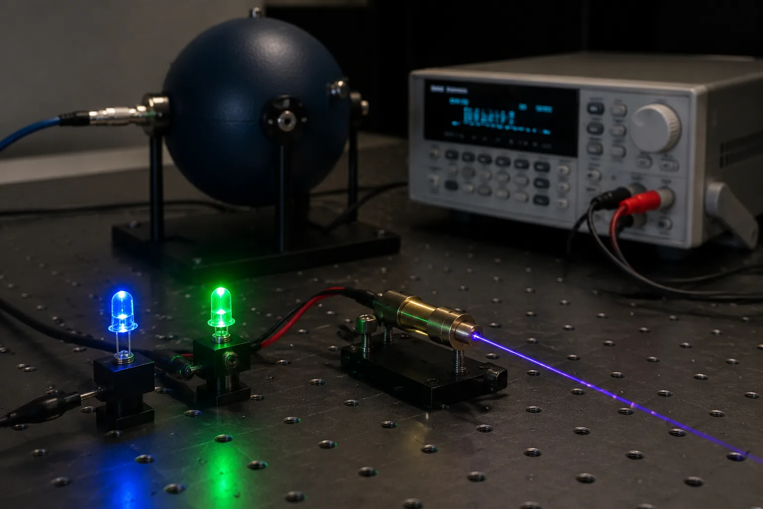
Why Optoelectronic Testing Is Different From Pure Electronic Testing
An optoelectronic device is a semiconductor junction that emits or detects light, so it must be characterised on both the electrical and the optical axes simultaneously — and the two interact. Testing it as if it were a pure electronic component (forward voltage, reverse leakage, capacitance) misses the optical half; testing only the optical output misses the junction physics. The distinctive measurement instruments — SourceMeter SMU (4-quadrant source-measure unit for I-V/LIV curves), integrating sphere (total luminous/radiant flux), spectrometer/OSA (spectral distribution), photodiode + optical power meter (absolute optical power), beam profiler (near/far-field), and optical link emulator (fibre/free-space link disturbances) — exist precisely because of this electrical-optical coupling. A single instrument (e.g. the Keithley SourceMeter driving the device while a photodiode SMU records the optical output) often characterises both axes synchronously.
What Are the Core Device Categories and Their Tests?
| Device | What it does | Key tests |
|---|---|---|
| LED (light-emitting diode) | Emits incoherent light | Forward I-V; luminous/radiant flux (integrating sphere); spectral distribution; chromaticity (CIE x,y / CCT / CRI); spatial distribution; ESD sensitivity (IEC 61340 / human-body-model) |
| Laser diode (LD) | Emits coherent light | LIV curve (Light-Current-Voltage) + kink (d²L/dI²); threshold current; slope efficiency; spectrum (centre wavelength, SMSR); beam profile & divergence (M²); back-facet-monitor current; temperature dependence |
| Photodiode (PD) / APD | Converts light to current | Responsivity (A/W) vs wavelength; dark current; quantum efficiency; capacitance; response time (rise/fall); reverse I-V breakdown; noise (NEP, D*) |
| CCD / CMOS image sensor | 2D imaging | Dark current & DSNU; non-linearity; conversion gain; charge-transfer efficiency; quantum efficiency (QE); photo-response non-uniformity (PRNU); modulation transfer function (MTF) |
| Optocoupler | Electrical isolation + signal transfer | Current-transfer ratio (CTR); isolation voltage; IEC 60747-5-5 safety & test methods |
| PIC (photonic IC) | On-chip optical functions | Wafer-level / die-level passive-optical, active-optoelectronic, telecom/datacom and RF/DC testing |
A test report must name the device class because the parameter set and the standard differ by class — a LED report (flux, chromaticity) is not a LD report (LIV, M²) is not a PD report (responsivity, D*).
How Is the LIV / I-V Characterisation Performed?
For active emitters (LED, LD), the headline test is the LIV curve — Light output (L), drive current (I) and forward voltage (V) swept together — and it illustrates why a SourceMeter SMU is the right instrument rather than a simple current source. A full active-optoelectronic characterisation requires both forward and reverse I-V:
- Forward I-V — sweep forward current, measure V_F and simultaneously record optical output L via an integrating sphere / photodiode; build the L-I curve, the I-V curve, and the dL/dI (slope efficiency) and kink test (d²L/dI²) that flag the onset of laser kinks and COD (catastrophic optical damage).
- Reverse I-V — force a small, precise reverse current (e.g. 10 nA) and measure the breakdown voltage V_R without damaging the device, then force a sub-breakdown reverse bias and measure leakage current I_L. The leakage value often gates the device for further testing.
- Four-wire (Kelvin) + driven guard — high-current forward sweeps need remote voltage sense (4-wire) to remove lead-resistance error; low-level reverse-leakage measurements need the driven guard to neutralise leakage paths. Two-wire measurement at high current produces false V_F.
- DUT protection — the SMU's programmable voltage/current compliance, fast output-off to 0 V, and contact-check-before-energise are what protect delicate AlGaAs laser diodes and silicon APDs from electrostatic/thermal damage during test.
- Synchronised multi-instrument — two SMUs (one driving the device, one on a photodiode) are triggered synchronously via a trigger-link so the optical reading and the electrical reading are paired at each point; the same technique ensures the source is stable before an optical-spectrum-analyser reading.
What Are the Optical and Spectral Measurements?
Beyond the electrical-optical LIV sweep, the optical side carries its own measurement suite, instrumented for the purity of light:
- Spectral distribution — high-accuracy wavemeter, Fabry-Perot scanning interferometer, and grating spectrometer (Ocean Optics/Hamamatsu miniature, Ando/HP/Thorlabs OSA) measure centre wavelength, linewidth, SMSR and side-mode suppression.
- Spectrophotometry — 1 m f/7 monochromator (180–2500 nm), Agilent Cary 5000 UV-Vis-NIR spectrophotometer and integrating sphere measure spectral transmittance/reflectance over wide dynamic range, for optical filters, coatings, and coating air-vacuum spectral shift.
- Beam profile and divergence — near-field and far-field profiles, beam quality (M²), astigmatism, measured with an optical train or Shack-Hartmann sensor + CCD.
- Power / energy / stability / modulation response — calibrated power and energy meters, integrating sphere and radiometer for CW and pulsed sources; modulation/frequency response for high-speed telecom devices.
- Stray light / scatter (BSDF) — angle-resolved scatterometry (CASI scatterometer, Albatross TT 3D @532 nm) characterises the bidirectional scattering distribution function that drives instrument-level stray light.
- Surface form / wavefront / topography — laser interferometer (DynaFiz @633 nm, surface form and wavefront error), white-light interferometric microscope (sub-nm 3D surface topography) for surface-quality verification.
What Are the Reliability and Qualification Tests?
Optoelectronic devices carry the same life-and-environment qualification burden as electronic components, plus optical-degradation modes (COD, dark-line defects, facet oxidation). The reliability framework is:
- GB/T 33768-2017 — 通信用光电子器件可靠性试验方法 (reliability test methods for communication optoelectronic devices): the Chinese commercial-grade reliability standard covering burn-in, steady-state and cycling operating life, damp heat, temperature cycling, and mechanical stress.
- GJB 548C-2021 / MIL-STD-883 — for high-rel/space: the same microelectronic-device test methods (Method 1005 burn-in, 1010 temperature cycling, PIND, hermeticity) applied to optoelectronic devices, plus optoelectronic-specific tests.
- GB/T 15651.4-2017 — semiconductor laser device ratings, characteristics and test methods.
- Long-duration endurance — month-long automated endurance testing in representative operational conditions (ESA-style), laser-diode accelerated-lifetime testing, and laser-induced-damage-threshold (LIDT) / laser-induced-contamination (LIC) screening for high-power laser optics.
- Environmental / space effects — thermal-vacuum, radiation effects on optoelectronic devices, and coating spectral-shift across the air-vacuum transition.
What About PIC (Photonic Integrated Circuit) Testing?
A growing share of "optoelectronic device" testing is photonic IC (silicon-photonics, InP) testing — the optical analogue of electronic IC testing. AIM Photonics (the US PIC foundry) defines the service as on-wafer, die-level and packaged PIC testing across four test domains — passive optical, active optoelectronic, telecom/datacom, and RF/DC — using 30+ tools at the TAP facility. The distinctive challenge is optical coupling to the chip: grating-coupler or edge-coupler alignment with sub-micron precision (Thorlabs NanoTrak auto-alignment, 3-axis NanoMax piezo stages), and the coupling loss / low efficiency that make wafer-level PIC testing far harder than electronic wafer probing. Micro-LED high-density arrays (pixel pitch ~10 µm) add the need for high-resolution, high-magnification microscopy and precision probe/probe-holder positioning.
What Belongs on the Report?
A compliant optoelectronic device test report states the device class, the parameter set measured, the standard and method (e.g. SJ/T 11394 LED method; GB/T 15651.4 laser; GB/T 33768 reliability; MIL-STD-883 / GJB 548C high-rel), the test conditions, and the result against the datasheet/acceptance criterion. For emitters the LIV + spectral + beam-profile data are the headline; for detectors the responsivity + dark current + QE + noise; for sensors the dark-current/DSNU/PRNU/MTF; for PICs the on-wafer / die / packaged test domain. Conflating device classes — reporting LED flux parameters against a laser datasheet — is a common error.
For the related laser-product safety service, see laser equipment testing per IEC 60825-1 / GB 7247-1; for the electronic-component counterpart, Electronic Component Testing.
FAQ
What is the difference between optoelectronic device testing and laser-equipment safety testing?
Optoelectronic device testing characterises the component (LED, LD, PD, sensor, PIC die) for electrical-optical performance and reliability — its LIV, responsivity, spectrum, MTF, reliability. Laser-equipment safety testing (IEC 60825-1 / GB 7247-1) tests the finished product (a laser system) for accessible-emission safety classification. The two are complementary: one qualifies the device, the other certifies the product.
Why does an LED or laser diode need both forward and reverse I-V testing?
Forward I-V gives the operating point, the L-I optical curve, slope efficiency and the kink test that catches COD; reverse I-V gives the breakdown voltage and leakage current that qualify the junction — leakage is often the gate that decides whether the device proceeds to further testing. A simple current source cannot characterise the reverse breakdown without risking damage; a 4-quadrant SourceMeter SMU can, which is why it is the standard instrument.
What is an LIV curve, and what does the kink test detect?
The LIV curve plots Light output, drive current and forward Voltage in one sweep. The kink test is the second derivative d²L/dI² — a sudden change in the slope of the L-I curve flags the onset of a "kink" (a non-linearity in light output), which is an early indicator of laser-diode degradation and catastrophic optical damage (COD). A smooth dL/dI across the operating range is the pass criterion.
Which Chinese standards govern optoelectronic device testing?
The GB/T 15651 national series (identical adoption of IEC 60747-5) covers LEDs, laser devices, photodiodes, optocouplers; SJ/T 11394-2009《半导体发光二极管测试方法》 is the LED test-method industry standard (with SJ/T 11577 application guide); GB/T 33768-2017 governs communication-device reliability; GB/T 15651.4-2017 covers semiconductor lasers. For high-rel/space, GJB 548C-2021 / MIL-STD-883 apply.
Can the same test bench cover LED, laser diode and photodiode testing?
The SourceMeter SMU, integrating sphere, spectrometer and beam profiler are shared infrastructure, but the parameter set, the standard and the acceptance criterion differ by device class (LED flux/chromaticity vs LD LIV/M² vs PD responsivity/D*). Each device class needs its own validated test method — a LED method is not a LD method.
Our Testing Capabilities
As an ISO/IEC 17025-accredited third-party laboratory, Beijing ZKGX Research provides optoelectronic device testing across the device classes and both the commercial and high-reliability frameworks:
- LED characterisation — forward I-V, luminous/radiant flux (integrating sphere), spectral distribution, chromaticity (CIE x,y / CCT / CRI), spatial distribution, ESD sensitivity, to SJ/T 11394-2009 / GB/T 15651 / IEC 60747-5-6.
- Laser diode characterisation — LIV curve + kink test (d²L/dI²), threshold current, slope efficiency, spectrum (centre wavelength, SMSR), beam profile and M², back-facet-monitor current, temperature dependence, to GB/T 15651.4-2017 / IEC 60747-5.
- Photodiode / APD characterisation — responsivity vs wavelength, dark current, quantum efficiency, capacitance, rise/fall time, NEP/D*, reverse-I-V breakdown, to GB/T 15651.7 / IEC 60747-5-7.
- Image sensor (CCD/CMOS) — dark current & DSNU, non-linearity, conversion gain, CTE, QE, PRNU, MTF.
- Optocoupler — CTR, isolation voltage, to GB/T 15651.5 / IEC 60747-5-5.
- Reliability / qualification — burn-in, operating life, damp heat, temperature cycling, mechanical stress, to GB/T 33768-2017 and GJB 548C / MIL-STD-883 for high-rel/space.
- PIC and micro-LED array — wafer-level / die-level / packaged passive-optical, active-optoelectronic, telecom/datacom and RF/DC testing, with sub-micron optical-coupling alignment.
Sample types include bare LED/LD/PD chips and dies, packaged devices, image sensors, optocouplers, photonic ICs, micro-LED arrays, and fibre-optic transceivers. If you have a specific device class, standard (IEC / GB / SJ-T / GJB / MIL-STD), application (telecom / display / sensing / space / automotive), or test domain (LIV / spectral / reliability / PIC wafer-level), contact the laboratory to confirm the exact test set and reporting format before testing.